


As the transmission of videos and other large-size data is becoming increasingly more common, the demand for the higher-capacity communication has risen. In order to meet this demand, NICT and SOC worked together to develop a device ideal for high-speed data transmission. More than ever, node technology and the means for transferring data itself carry great importance for high-speed data transmission. If one were to compare an optical communication system to a highway, the transmission technology would represent the performance of the roads themselves, such as the number of the lanes. On the other hand, the node technology corresponds to capacity of the interchanges of helping to keep the flow of vehicles bound for various destinations running smoothly. Thus, in order to elevate the performance of the system as a whole, it is essential to improve not only transmission technology but also node technology. NICT has been conducting research on optical packet systems, seeking to develop efficient nodes. One of the key technologies supporting the superior performance of optical packet nodes is the optical switching device. Normally, guard time is allotted to secure the time needed for controlling optical signal destinations. However, with conventional switching devices, enhanced data transfer rates cause guard times to become increasingly longer than the time effectively used for sending data. As a result, data processing capacity at the node degrades considerably.
Home > Press Release > A Guard-Time-Free High-Speed Switching for Optical Signals
- Eliminating Communication Bottlenecks by Switching the Destinations of Optical Signals in a Fraction of a Second -
The National Institute of Information and Communications Technology (NICT, President: Hideo Miyahara) and Sumitomo Osaka Cement Co., Ltd. (SOC, President: Yutaka Watanabe) have succeeded in developing a high-speed optical switching device. This device enables optical signals to be switched at incredibly high speeds, at a rate of 10 Gbit/s (gigabit per second). Likewise, there is no guard time, or time used for switching operations, during which no data is sent. This new device is 100 times faster and more precise than its predecessor, achieving a switching time as short as 26 ps.
We have been conducting research on high-speed optical switching devices and recently achieved an instantaneous changeover (switching time of 26 ps) of optical signal destinations, using control technology and a newly created optical integrated circuit. Compared to traditional, commercially available optical switching devices made with similar materials, the switching precision measured by the extinction ratio (the ratio of desired signal and unwanted signal) is 100 times more precise, and the switching speed is more than 1,000 times faster. We have demonstrated that, using this new device, the high-speed 10Gbit/s signals can be switched without leaks and guard times. We have also confirmed that there is minimal signal degradation when switching is performed, as well as no signal errors.
This year, we presented the breakthrough results of our experiments at the Optical Fiber Communication Conference and Exposition (OFC), and the National Fiber Optic Engineers Conference (NFOEC), the latter being held between March 22nd and March 26th, in San Diego, U.S.A.
As part of our contribution to society, we continue to develop optical network system technologies, seeking to make devices smaller and less expensive. We are also working to integrate these technologies with other next-generation high-speed transmission technologies. We firmly believe that this newly developed device will play an important part in helping to meet the large demand for future networking technology.
Gbit/s (gigabit per second)
A gigabit per second is a unit of measure for data transfer and processing. A bit (one or zero) is the smallest unit of measure for digitized information. One gigabit is equal to one billion bits. One Gbit/s means the capacity for sending or processing data is one gigabit per second.
Guard time
The necessary time interval for controlling the optical switch, as well as the time needed for system synchronization. During a guard time data transfer is halted. Reducing guard times is one of the major challenges when seeking to improve data transfer and processing rates.
ps (picosecond)
A unit used to measure an extremely short period of time. One picosecond is equal to one trillionth of a second.
Node technology
Technology for controlling the various destinations of the data.
Optical packet
In a packet exchange network, data is formatted into “packets.” A destination information (label) is attached to each packet, and this information is used when exchanging packets. Optical packet technology allows packets to be processed and exchanged as optical signals, without converting them into electrical signals.
Commercially available optical switching devices
The operation speed of the conventional optical switching devices commonly used in current systems is considerably slower than this newly developed device. The fastest products take more than 1 millisecond (a thousandth of a second) for switching. Compared to a conventional product with a common switching time of 1 millisecond, our new device promises to be 30 million times faster. Thus, we can conclude that the optical signal destinations are switched practically instantaneously.
The devices we refer to when drawing comparisons are all made of the same material (lithium niobate) as our newly developed device. Likewise, these comparison models possess the highest operation speeds for all commercially available devices.
Appendix
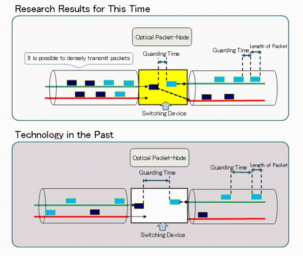
When the guard time required for switching becomes longer than the length of the packet, the efficiency of data transfer/processing deteriorates. Thus, it is imperative to shorten the guard time within the high-speed optical packet system.
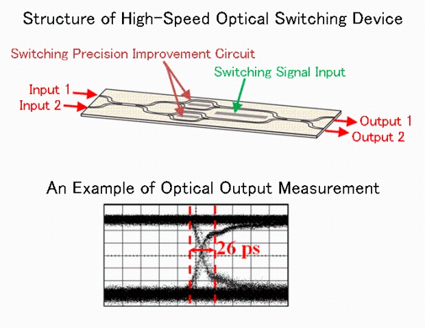
The device has two pairs of input and output terminals, and can switch between the following two states: Input 1 and Output 1. Input 2 and Output 2 are connected respectively. Input 1 and Output 2, and Input 2 and Output 1 are connected respectively. The main features are the switch signal input, and the switching precision improvement circuit. The measured switching time was 26 ps.
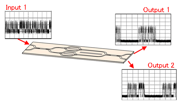
The optical signal added to the Input 1 is separated to two different destinations (Output 1 and Output 2) at a specified time. The length of the guard time allowed for switching is zero. We effectively demonstrated that error-free switching, with no leaks, is possible.
Technical Contact
Akito CHIBA and Tetsuya KAWANISHI
Lightwave Device Project
Advanced Device Research Group
New Generation Network Research Center, NICT
Tel :+81-42-327-7490
Yuji ISEKI
Design and Marketing Group
New Technology Research Center
Sumitomo Osaka Cement Co., Ltd.
Tel :+81-47-457-0195
Press Release Contact
Sachiko HIROTA, Specialist
Plublic Relations Office
Strategic Planning Department
NICT
Tel :+81-42-327-6923
Hitoshi KIMATA
IR Publicity Group
General Affairs Department
Sumitomo Osaka Cement Co., Ltd.
Tel :+81-3-5211-4964