Article
Font Size: SmallerFont Size: DefaultFont Size: Larger
  • 日本語トップ

Big Step toward Practical Use of Leading-edge “Optical Packet and Circuit Integrated Network”

- Manufacturing Practical Optical Nodes from the Latest Optical Switching Technologies and Building the World’s First Testbed -

  • Print this page
June 14, 2011

National Institute of Information and Communications Technology (NICT, President: Dr. Hideo Miyahara) has built the world’s first testbed environment for high practicality “optical packet and circuit integrated network” by bringing together the world’s highest level of NICT’s optical switching technologies.

The successfully developed “optical integrated node equipment” can make remarkably stable operation even under the real network environment, and it is so easy to operate and conduct verification tests on a new optical network that the operators are not necessarily specialists on optical hardware units.

Active utilization of this testbed contributes strongly to the realization of “the optical packet and circuit integrated network” that can make an efficient use of the communication lines as well as ensure the communication quality.

Background

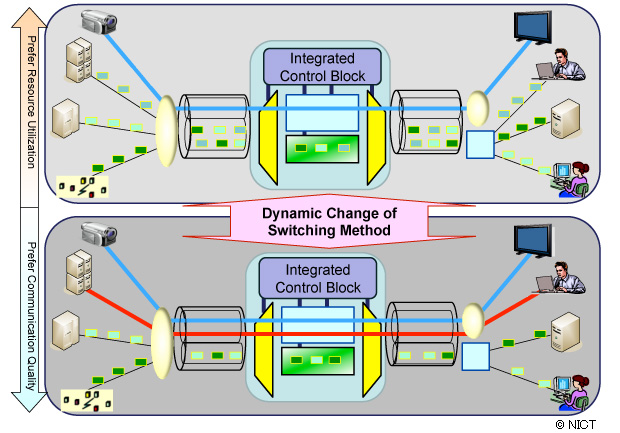
NICT has been conducting advanced research since 2008 on the “optical packet and circuit integrated network technology” (Fig. 1) , which enables users to make a flexible choice in either high-speed and low-cost service or high-quality service without delay and data-loss based on their usage scenes, and last year NICT succeeded in verification test with the optical packet and circuit integrated proto node.

In the previous optical integrated proto node being simply put individual lab equipment, however, it was difficult to conduct verification tests under the real network environment since the equipment behaves in an unstable way by the influence of rapid changes in the packet flow interval or temperature variation especially in the optical packet network. Testing with using such an unstable node equipment required high technical knowledge about optical units and also required operations by networking experts even when setting up the network data transfer control. Therefore, NICT has been working to develop the equipment that can conduct verification tests in the real environment for the realization of “optical packet and circuit integrated network”.

New Achievements

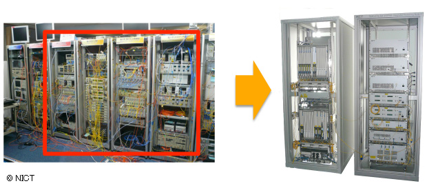
This time, NICT has succeeded in developing the new “optical packet and circuit integrated node equipment” with superior stability and operability by bringing together research outcomes of the latest optical packet switching technologies (Fig. 2). The equipment ensures less than half size in chassis compared to the previous one. In addition, the quality of the optical packet at receiver side fully satisfies the tough ITU-T standards at all times in terms of packet error rate (PER) and there was very little equipment adjustment required, even in the real environment where a stable behavior could not be assured with the previous equipment. The total number of hours for equipment adjustment to ensure the stable experiment environment could also be reduced by approximately 90% of that of the previous one. These achievements allow both those who have no expertise in optical units to manipulate the unit by themselves and network operators to make an easy control setting even when there is some change in test composition, including an increase in the number of units in the network.

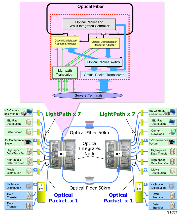
This test environment was established as part of the supplementary budget “Maintenance of Verification Infrastructure for Optical Switching Technology” for fiscal year 2009, administered by the Ministry of Internal Affairs and Communications (Fig. 3).

Future Plans

In order to further enhance the function of the optical integrated node equipment, we will make continued research and development in the introduction of optical buffer function as well as higher functionalization and automation of the data transfer control unit, and we will also work toward the practical use of the reliable “optical packet and circuit integrated network” that is easily available to more users and network administrators. We will further develop the new generation network with the use of this achievement as our JGN-X testbed infrastructure.

This successful achievement was lively demonstrated at the Interop Tokyo 2011 being held at the Makuhari Messe International Convention Complex from June 8 to 10, 2011.  

Fig. 1  Overview of NICT's optical packet and circuit integrated network
Fig. 1 Overview of NICT's optical packet and circuit integrated network


Each node transfers data on packet line or circuit line flexibly according to the user request.

Fig. 2  A node equipment for an optical packet and circuit integrated network
Fig. 2 A node equipment for an optical packet and circuit integrated network
(Left: previous proto node  Right: a new node equipment)


The previous proto node needs 4 or more shelves of space.
The new node equipment needs half or less than the previous one by device stabilization and integration.

Fig. 3  Diagram of the node equipment and verification environment
Fig. 3 Diagram of the node equipment and verification environment


Node equipment that we have been developing this time is mainly used for a ring network. This has the following functions as well as optical transceivers and optical packet switches.

  • Optical drop function that demultiplexes data received from a ring network.
  • Optical add function that multiplexes data from client to a ring network.
  • Transfer data coming from fiber in a ring network to another fiber without drop.
We built a verification environment in which a network consists of two optical packet and circuit integrated nodes we developed this time. The distance between two nodes is 50km. We verified uncompressed 4K movie transfer over 100Gbps optical packet line and high-speed file transfer and uncompressed high-definition video transfer over lightpaths (7 lightpaths in this experiment). The performance was stable. This live demonstration was operated in Interop Tokyo 2011 at NICT booth.

Technical Contact

Naoya Wada

Photonic Network System Laboratory,
Photonic Network Research Institute

Tel:+81-42-327-6371
E-mail:

Hideaki Furukawa

Network Architecture Laboratory,
Photonic Network Research Institute

Tel:+81-42-327-5694
E-mail:

Media Contact

Sachiko Hirota

Public Relations Department

Tel:+81-42-327-6923
E-mail: