Article
Font Size: SmallerFont Size: DefaultFont Size: Larger
  • 日本語トップ

High-Precision Wavelength-Tunable “Quantum Dot Light Source” in World’s First Developed by Nanotechnology

- Pave Way for Ultra-High-Speed, High-Capacity Optical Communication using New Frequency Band -

  • Print this page
December 26, 2011

The National Institute of Information and Communications Technology (NICT President: Dr. Hideo Miyahara) has succeeded, for the first time in the world, in developing an optical source for generating light of a large number of wavelengths with high precision. This was made possible by employing semiconductor quantum dots of nanoscale structure in a band consisting of wavelengths that are not currently used for optical communication. Further, we have succeeded in conducting an optical transmission experiment using this light source and a photonic crystal fiber, which demonstrated the possibility of using a new wavelength band for optical communication for the first time.

The “quantum dot light source technology” makes it possible to secure an optical frequency resource (about 70 THz) whose band covers about 10 times the width of the currently used optical communication wavelength band. This improves the band’s efficiency. Moreover, as quantum dots and a photonic crystal fiber have nanoscale structures, the application of nanotechnology is expected to be a revolutionary technology for an optical information communication.

The Details of this achievement were published in “Optics Express” by the Optical Society of America on December 12, 2011.

Background

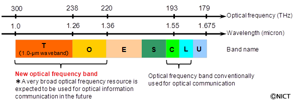
The current optical fiber communication systems use a 1.55-micron wavelength band of about 10 THz, where the attenuation of the optical signal and distortion of data are quite low (See Fig. 1). Although research and development for an efficient use of the optical signal in this wavelength band has been in progress, these measures alone are not sufficient for bringing the ultra-high-speed and the large-capacity optical communication in the future into reality, due to lack of frequency resources.

For this reason, NICT has engaged in a basic technology research related to development and efficient use of optical frequency resources by employing photonics-based technology for an effective utilization of the optical frequency band in the broadband region, where it is difficult to use for transmission or for generation of light (See Fig.1). Therefore no other research and development has been carried out so far.

New Achievements
High-precision wavelength-tunable quantum dot light source

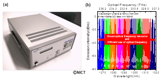
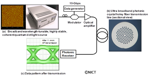
By employing semiconductor quantum dots as optical amplifying material acting in the 1.0–1.3 micron wavelength band, NICT has succeeded in developing a quantum dot light source with a combination of stability and a high optical frequency. This leads to the tunability of the broadband wavelength and the effective use of the optical frequency (See Fig. 2). In order to develop the quantum dot material, which is the key to the light source, NICT has used a self-developed “subnanometer interlayer separation technique” (See Fig. 3) which controls the crystal structure at an atomic level (subnanometer level). That way, we have achieved a high quality and a high density that is twice of that achieved conventionally. Moreover, we have succeeded in building a high-speed data transmission system (See Fig. 4) with error-free data transmission that combines this light source and the photonic crystal fiber with ultra-broadband optical propagation characteristics.

Future Prospects

By applying the quantum dots and the photonic crystal fiber technology as the basic technology for the optical network components, an enormous expansion of the optical frequency resource useful for communication of optical information is expected. It is also expected that an effective use of the optical frequency brings a technological revolution. Furthermore, as this new wavelength band (1.0–1.3 micron band) proves excellent permeation through human skin and moisture, applications in bioimaging or medical sensing are expected.

A prototype of the “quantum dot light source”, developed by NICT, has been designed by Koshin Kogaku Co. Ltd. and Sevensix, Inc. The technology transfer and development for commercialization of the product is being under way.

The Details of this achievement were published in “Optics Express” (Vol. 19, Iss. 26) by the Optical Society of America on December 12, 2011.
 (http://www.opticsinfobase.org/oe/abstract.cfm?URI=oe-19-26-B636)

Appendix

Fig. 1: A Relationship of band names allotted to optical communication with a optical frequency (wav
Fig. 1: A Relationship of band names allotted to optical communication with an optical frequency (wavelength) band

The C band (about 4 THz wide) and L band (about 7 THz wide) of the 1.55-micron wavelength band are used the most as the optical communication bands. Enormously broad optical wavebands are expected in the T band and O band (about 70 THz wide) of the 1.0–1.3 micron waveband, which is now the focus of attention.

Fig. 2 : A quantum dot light source newly developed

(a) An optical source using high-quality quantum dots as light-amplifying material
(b) An example of the wavelength tunability of the quantum dot light source 

The world’s longest wavelength for optical communication, 1300 nm (1.3 μm), has been achieved in the form of low-cost quantum dots with a large surface area on a GaAs (gallium-arsenic) semiconductor base. A high optical frequency stability has also been realized, leading to an effective use of the broadband wave-tuning property at optical frequencies.

Fig. 3 : A Subnanometer interlayer separation technique

(a) A sectional diagram of subnanometer interlayer separation technique
(b) Left: A quantum dot structure developed using the conventional technique
Right: A high-quality quantum dot structure newly developed
(c) A quantum dot optical gain device

The interlayer separation technique originally developed by NICT has a structure where a crystal of atomic size (with a subnanometer length) is sandwiched between a quantum dot and a quantum well (a).

In this technique, the structure of the quantum dots does not involve large aggregates leading to deterioration of the crystal properties or light amplification characteristics, in contrast to the conventional technique (Fig. b, left). We have succeeded in preparation for a semiconductor (Fig. b, right) of the world’s highest quality and density, which is more than two-fold higher than that achieved conventionally.

The device in (c) consists of the broadband wavelength-tunable, narrow-line-width quantum dot light source newly developed.

Fig. 4 : A high-speed optical propagation subsystem

The optical transmission subsystem was built using the combination of the two components in (a) and (b).

By applying nanotechnology, the possibility of using a new optical frequency band in an optical information transmission network has been demonstrated for the first time (c).

Glossary

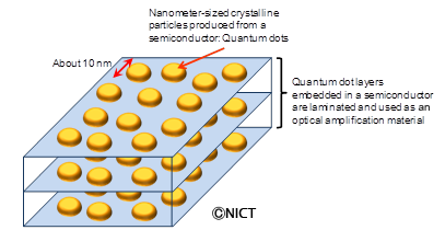
A quantum dot is a tiny particle of nanometer scale made of semiconductor crystals. Use of this minute structure as a luminescent material or light-amplifying material in optical devices enables broadband operation at longer wavelengths, which is difficult to achieve by conventional means. Optical devices using quantum dot structures are expected to have a low environmental load, making this a green technology with low power consumption. Moreover, applications of quantum dots in solar batteries and quantum information communication technology are also expected.

A bird’s-eye view of a quantum dot structure used as a light-amplifying material

The nano- (n) prefix indicates 1/1,000,000,000. One nanometer is approximately equal to the size of 10 atoms.

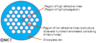
A photonic crystal fiber is an optical fiber with regular and periodic holes near a core region that allows propagation of light. This fiber allows propagation of light in a broader waveband than allowed by a conventional optical fiber, and it has the ability to withstand high input power, is sturdy against bending, and has the wiring flexibility to withstand bending. A holey fiber is a typical example of the photonic crystal fiber.

The tera- (T) prefix indicates 1 trillion.

Nanotechnology
The size of atoms or molecules is measured in nanometers, and nanotechnology is a field involving development of techniques with accuracy on the order of nanometers. With the full utilization of nanotechnology, development of new materials with properties that are not found in conventional materials will become possible, which will improve performance of electronic devices. Nanotechnology is expected to have applications in many fields, such as materials technology, industry, medicine, and environmental technology.

A sectional view of a holey fiber

An optical fiber is composed of a region with a high refractive index (core) and its surrounding region with low refractive index (clad). The core region allows propagation of light.
In a holey fiber, the clad consists of a number of holes. The properties of the optical fiber can be improved by adjusting the size, distribution, or shape of the holes on the nanoscale..


Technical Contact

Naokatsu Yamamoto, Koichi Akahane,
Tetsuya Kawanishi

Lightwave Devices Laboratory
Photonic Network Research Institute
Tel: +81-42-327-7453
E-mail:

Media Contact

Sachiko Hirota

Public Relations Department
Tel: +81-42-327-6923
E-mail: