


This work was partially supported by “The research and development project for innovation technique of energy conservation” of the New Energy and Industrial Technology Development Organization (NEDO).
Home > Press Release > First Demonstration of Gallium Oxide (Ga2O3) Metal-Oxide-Semiconductor Field-Effect Transistors (MOSFETs)
First Demonstration of Gallium Oxide (Ga2O3) Metal-Oxide-Semiconductor Field-Effect Transistors (MOSFETs)
- Japan Paves the Way for Practical Applications of Next-Generation Innovative Power Devices -
June 19, 2013
The National Institute of Information and Communications Technology (NICT, President: Dr. Masao Sakauchi), in collaboration with Tamura Corporation (Tamura, CEO: Naoki Tamura) and Koha Co., Ltd. (Koha, CEO: Yasuhiro Nakashima), has developed gallium oxide (Ga2O3) metal-oxide-semiconductor field-effect transistors (MOSFETs).
Ga2O3 is a promising new semiconductor material for high-breakdown and low-loss power devices. Its excellent material properties, such as wide bandgap, can reduce the cost and energy consumption of power conversion. Ga2O3 power devices can be fabricated on native melt-grown single-crystal substrates, leading to a great advantage of Ga2O3 over other widegap semiconductors such as SiC, GaN, and diamond for low-cost mass production. The Ga2O3 MOSFETs have a structure and characteristics applicable for actual use as is. We expect that the development of Ga2O3 power devices will not only alleviate global energy problems but also play an important role in the semiconductor industry in the near future.
Details of this achievement will be presented at the 2013 Device Research Conference (DRC2013), which will be held from June 24th to 26th at the University of Notre Dame, USA.
Background
The worldwide quest for innovative technologies beyond Si for efficient power switching has led to the development of high-breakdown and low-loss power devices using widegap semiconductors such as SiC and GaN. We envision that gallium oxide (Ga2O3) will be even more competitive than SiC and GaN for power devices because of its wider bandgap and other superior material properties. Another potential benefit of Ga2O3 is that native single-crystal substrates can be mass-produced by the melt-growth method. However, R&D on Ga2O3 electrical devices has lagged in spite of the material’s high potential.
New Achievements
We fabricated Ga2O3 metal-oxide-semiconductor field-effect transistors (MOSFETs), which are the most suitable FET structures for practical applications. Highlights of this development are novel technologies of ion implantation doping and gate dielectric deposition. The Ga2O3 MOSFETs exhibited excellent device characteristics including (1) a high on-state drain current (39 mA/mm), (2) a large off-state breakdown voltage of 370 V, (3) an extremely low leakage current (less than a few pA/mm, which was the lower detection limit of the measurement instrument), and (4) a high on/off drain current ratio of over 10 orders of magnitude. These excellent device characteristics will lead to a large reduction in power loss during switching operations and will be suitable for practical power devices.
Future Prospects
This development of MOSFETs using the new widegap semiconductor Ga2O3 will pave the way for new high-performance power devices in both high- and low-voltage applications, contributing not only directly to the global energy savings but also to the economy of Japan by opening up new opportunities in the semiconductor industry. We anticipate that R&D on Ga2O3 power devices will be of global interest.
Appendix
 Prospective applications of power semiconductor transistors (b) Benchmarking the ideal performance limits of Ga2O3 against other representative semiconductors")
Fig. 1:(a) Prospective applications of power semiconductor transistors
(b) Benchmarking the ideal performance limits of Ga2O3 against other representative semiconductors
Figure 1(a) shows the prospects of Ga2O 3 and other power semiconductors as predicted from their material properties. Ga2O3 power devices will initially be targeted toward high-voltage and high-power applications. As Ga2O 3 devices become more established, their applications will broaden to those of SiC and GaN by virtue of their simple and low-cost substrate production.
The performance of power devices is characterized by their on-resistance and breakdown voltage. A tradeoff relationship exists between these two parameters, whereby enhancing the breakdown voltage of the devices to realize high-voltage utilization necessarily increases their on-resistance and hence power loss in the form of heat generation. The ideal performance limit of Ga2O3 power devices is benchmarked against those of other representative power devices in Fig. 1(b), according to which the bottom-right corner represents better device performance. We can see from this estimate that Ga2O3 transistors are less lossy (i.e. more energy-efficient) than Si and SiC transistors at a given breakdown voltage by ~3,000 and ~10 times, respectively. The reduction in power loss corresponds directly to the amount of energy saved. Therefore, Ga2O3 has better characteristics as a power device material than not only Si but also SiC and GaN.

Fig. 2: 2-inch-diameter single-crystal β-Ga2O3 substrate fabricated by the melt-growth method
Figure 2 shows a photograph of a 2-inch-diameter single-crystal β-Ga2O3 melt-grown substrate. The melt-growth method is a low-energy-consumption, low-cost way of making large substrates because it does not require a high-temperature and/or high-pressure environment and uses less source material. As the substrate production cost accounts for a large percentage (~60%) of the total production cost of widegap power devices (SiC, GaN, and diamond) for which a melt-grown substrate technology is unavailable, the ability to mass-produce large area single-crystal substrates from a melt is a huge cost advantage of Ga2O3 over other widegap semiconductors. We anticipate that a large Ga2O3 substrate (over 6~8 inches in diameter) will cost at least 10-100 times less than SiC and GaN substrates.
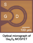
 Cross-sectional schematic illustration and (b) optical micrograph of Ga2O3 MOSFET")
Fig. 3:(a) Cross-sectional schematic illustration and (b) optical micrograph of Ga2O3 MOSFET
Figures 3(a) and (b) show a schematic cross-sectional illustration and an optical micrograph, respectively, of a Ga2O3 MOSFET fabricated using the new device process technologies of (1) selective-area ion implantation doping and (2) dielectric film deposition.
 Output and (b) transfer characteristics of Ga2O3 MOSFET")
Fig. 4:(a) Output and (b) transfer characteristics of Ga2O3 MOSFET
Figure 4(a) shows the output characteristics of the Ga2O3 MOSFET. Effective gate control over the drain current was evident. Furthermore, the off-state breakdown voltage was 370 V, a very high value considering the fact that the device consisted of a simple FET structure without incorporating any techniques to increase the breakdown voltage. As shown in Fig. 4(b), the off-state drain leakage current was very small (a few pA/mm, which was less than the lower limit of the measurement instrument), resulting in a high on/off drain current ratio of over ten orders of magnitude. The low leakage current in the off state directly leads to low power loss.
The combination of material properties superior to other semiconductors’, high quality single-crystal substrates, and novel process technologies developed in this work have led to the excellent devices characteristics of Ga2O3 MOSFETs. Despite a simple transistor structure, these devices have already satisfied the requirements for practical applications.
Technical Contact
Masataka Higashiwaki
Advanced ICT Research Institute
Tel: +81-42-327-6092
E-mail: 


Media Contact
Sachiko Hirota
Public Relations Department
Tel: +81-42-327-6923
E-mail: 


