
In the Advanced ICT Device Laboratory, we have processing rooms that are kept in a cleanroom environment and free from dust. The processing rooms are equipped with utilities and apparatus groups for use in various processing and measurements. Possible operations include drawing of ultra-fine patterns with an electron beam or light source, formation of high purity films with molecular beams or plasma, ultrafine processing with a focused ion beam, formation of electrodes and connecting of optical fibers, and observation of micro shape of materials and element analysis using an electron microscope. Users of our facilities can produce, study, and develop prototypes of photonic and millimeter-wave devices using semiconductor and dielectric materials. Our veteran technical staff maintain the utilities and apparatus in appropriate conditions for use under a system which provides standard use conditions for all users of individual facilities. We are making our best efforts for safety and disaster prevention measures and environment protection. We fully consider treatment of industrial wastes, exhaust gas, wastewater, noise, and other problems. We provide the environment in which users can concentrate on production, study, and development of prototypes of photonic and millimeter-wave devices.
Message
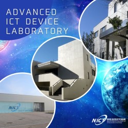
Background
Feature of the Laboratory
Laboratory Management and Use by Other Entities
Paid Utilization System: NICT Open Facility Information
History
|
A meeting of investigation committee of the Photonic Device Center held. |
October, 1998 |
|
The report “Survey and Study on the Significance of Research on Photonic Information and Communication Devices in CRL (Communications Research Laboratory)” submitted. |
March, 1999 |
|
A request “Establishment of the Photonic Device Research and Development Center (tentative name)” submitted. |
April, 1999 |
|
Investigation on the conditions required for a cleanroom conducted. |
January, 2000 |
|
Construction of the Photonic Technology Center started. |
March, 2001 |
|
Operation of cleanrooms started. |
May, 2001 |
|
Installation of MBE and other apparatus and their operation started. |
June, 2001 |
|
Repair work on facilities of Photonic Device Technology Center finished. |
July, 2002 |
|
Installation of apparatus for use in device manufacturing |
July, 2003 |
|
The WWW site of the Photonic Device Technology Center opened. |
February, 2004 |
|
A forum for the Photonic Device Technology Center held. |
February, 2004 |
|
A call for proposals for collaborative research |
October, 2004 |
|
The center renamed to “Photonic Device Laboratory”. |
May, 2006 |
|
Certification of ISO14001 regarding environmental management system of the laboratory, examined and registered. |
February, 2007 |
|
The laboratory renamed to “Advanced ICT Device Laboratory”. |
April, 2012 |
|
Certification extension (renewal) of ISO14001 for environmental management system on the laboratory, examined and registered. |
December, 2012 |
|
Start operation of new utilities and apparatus |
April, 2014 |
Efforts toward Environment Management
Background of ISO14001 Certification of the Advanced ICT Device Laboratory
|
Dec. 2006 |
Preparation phase |
|
|
|
Investigation on the current condition of the laboratory |
|
|
Jul.-Aug. 2006 |
Reestablishment of the environmental management system |
|
|
An instruction manual for the laboratory environment created. |
||
|
The environmental management system promotion committee organized. |
||
|
An organization framework for the environmental management developed. |
||
|
Photonic Device Laboratory Environmental Management Policy formulated. |
||
|
Planning on environmental management |
||
|
The environmental targets and goals decided. Implementation Plan for FY2006 started. |
||
|
Nov.10, 2006 |
Internal audit was performed. |
|
|
Nov. 30, 2006 |
Audits by an external agency for ISO14001 registration performed. |
|
|
Audit stage 1 passed. |
||
|
Feb. 7, 2007 |
Audit stage 2 passed. |
|
|
Feb. 26, 2007 |
Certification is given. |
|
|
Dec. 2012 |
ISO14001 renewal audit |
|
|
|
The audit performed subject to the Advanced ICT Device Laboratory as a whole, after integration of the functions associated with millimeter-wave devices. |
|
|
Feb. 2013 |
ISO14001 renewal registration |
|
|
|
ISO14001 certification for the Advanced ICT Device Laboratory as a whole |
|
|
Feb. 2017 |
ISO14001 renewal registration |
|
|
|
Transition to the ISO standard 2015 completed. Received the award for obtaining certification of environmental management system over a long term |
|
|
Summary |
The Advanced ICT Device Laboratory has established an environmental management system and obtained an ISO14001 certification. |
|
Registered name and address |
National Institute of Information and Communications Technology Advanced ICT Device Laboratory 4-2-1, Nukui-Kitamachi, Koganei, Tokyo 184-8795 |
|
Application scope |
- Photonic Device Laboratory - Millimeter-wave communication device research building (1st floor and 2nd floor; rooms for prototype manufacturing and evaluation of communications tools) |
|
Certifying organization |
JSA Solutions Co., Ltd. |
|
Registration No. |
JSAE 1317 |
|
Applied standards |
JIS Q 14001:2015, ISO 14001:2015 |
|
Certification scope |
(JAB approval scope number; 34) The environmental management system to promote; (1) Encouragement for the users to use the facilities in consideration of the environment, |
|
Initial certification date |
February 26, 2007 |