
World's First Practical Surface-Emitting Laser for Optical Fiber Communications Developed: Advancing Miniaturization, Energy Efficiency, and Cost Reduction of Light Sources
Highlights
-
Development of the world's first practical surface-emitting laser suitable for optical fiber communications systems.
-
Utilization of quantum dots as an optical gain medium, enabled by NICT's high-precision crystal growth technology and Sony's advanced processing technology.
-
A significant advancement toward miniaturization, reduced power consumption, and cost efficiency of light sources used in optical fiber communication systems.
The National Institute of Information and Communications Technology (NICT, President: TOKUDA Hideyuki Ph.D.), in collaboration with Sony Semiconductor Solutions Corporation (Sony), has developed the world's first practical surface-emitting laser that employs quantum dot(QD) as the optical gain medium for use in optical fiber communication systems.
This achievement was made possible by NICT's high-precision crystal growth technology and Sony's advanced semiconductor processing technology. The surface-emitting laser developed in this study incorporates nanoscale semiconductor structures called quantum dots as light-emitting materials. This innovation not only facilitates the miniaturization and reduced power consumption of light sources in optical fiber communications systems but also offers potential cost reductions through mass production and enhanced output via integration.
The results of this research were published in Optics Express, a leading international journal in optical technology, published by the OPTICA Publishing Group in the United States, in Vol. 33, Issue 6, on Monday, March 24, 2025.
Background
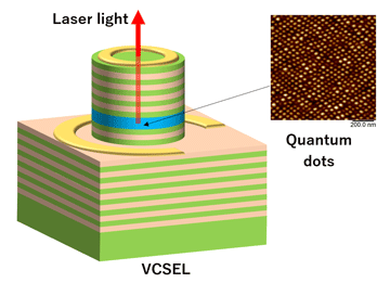
Figure 1. Schematic of a surface-emitting laser and guantum dots.
Modern communication technologies require large-capacity data transmission with minimal power consumption. Vertical-cavity surface-emitting lasers (VCSELs) have attracted significant attention as a key technology that addresses these requirements, particularly in optical communications. However, VCSELs typically operate in the near-infrared region, at wavelengths of 850 or 940 nm. Developing VCSELs that operate at the long wavelength of 1,550 nm—typically used in existing optical fiber communications—presents significant technical challenges. This challenge results from the increased complexity in both material selection and structural design for long-wavelength VCSELs than those of short-wavelength VCSELs. In addition, achieving high output and efficiency in VCSELs at 1,550 nm, it is necessary to develop a material or device structure that emits efficiently.
Achievements
In a joint research project with Sony, NICT achieved the world's first electrically driven VCSEL operating at 1,550 nm—the standard wavelength for optical fiber communication—using nanoscale semiconductor structures known as quantum dots as the optical gain material (see Figure 1).
NICT developed the first core technology: a high-precision crystal growth method for compound semiconductors using molecular beam epitaxy. Fabricating a VCSEL requires growing a highly reflective semiconductor multilayer film (DBR: Distributed Bragg Reflector) to enhance light intensity; however, fabricating DBRs that operate at 1,550 nm has been challenging because the combination of materials that can be grown is limited. In this study, we developed a technology that can precisely grow DBR by strictly controlling the ratio of materials in the crystal growth and realized a semiconductor DBR with a high reflectivity exceeding 99% even at 1,550 nm. In addition, strain-compensation techniques were applied to the VCSEL production to accurately cancel the internal crystal strain (strain generated within the material) that occurs around the quantum dots, thereby significantly increasing the density of the quantum dots and improving the light-emitting performance.
Sony contributed to the second core technology: a device design and fabrication process that enables highly efficient current injection employing a structure called a tunnel junction. VCSELs emit light perpendicular to the wafer surface; therefore, even if quantum dots emit light, conventional electrode placement obstructs light extraction. Sony addressed this by implementing a tunnel junction structure that permits efficient current flow while facilitating light extraction employing a precise device process.
Through the integration of these two technologies, we succeeded in lasing VCSELs using quantum dots at 1,550 nm as a light-emitting material with a small current of 13 mA (low threshold). Furthermore, polarization fluctuations were eliminated, resulting in a stable output.
VCSELs employing quantum dots as optical gain materials, exhibit excellent temperature stability. In addition, VCSELs exhibit scalable structures that enable mass production. These characteristics are expected to enable higher performance, reduced cost, and higher output via the integration of optical communication wavelength-band lasers.
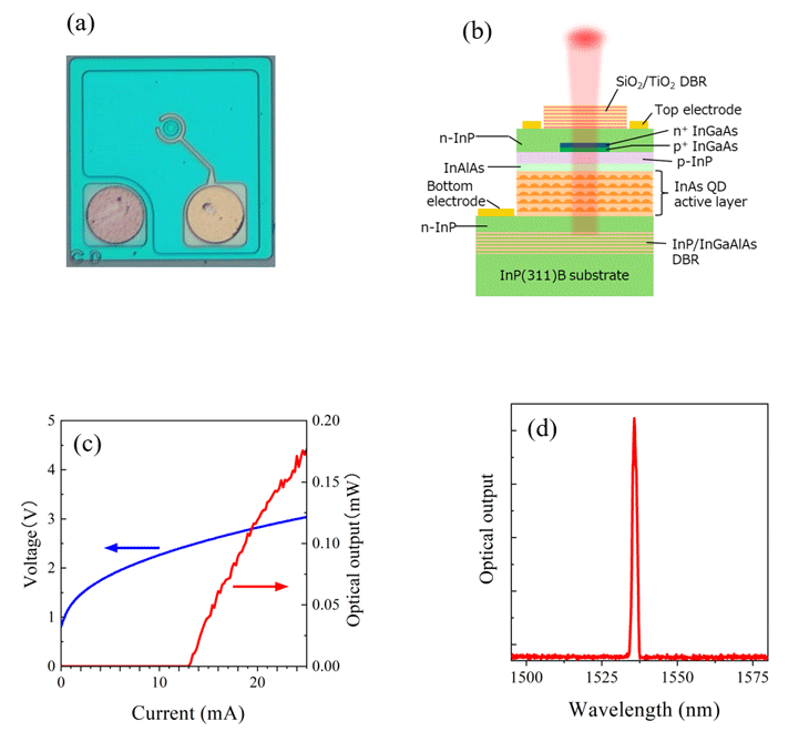
Figure 2 (a) Micrograph of the quantum dot-based VCSEL that was fabricated,
(b) Schematic of the cross-sectional structure of the quantum dot-based VCSEL,
(c) Current-light output characteristics (red) and current-voltage characteristics (blue), (d) Laser oscillation spectrum of the VCSEL.
(b) Schematic of the cross-sectional structure of the quantum dot-based VCSEL,
(c) Current-light output characteristics (red) and current-voltage characteristics (blue), (d) Laser oscillation spectrum of the VCSEL.
Future Prospects
We aim to conduct advanced technical studies on quantum-dot-based VCSEL technology to further enhance the capacity and reduce power consumption in optical fiber communication systems beyond the 5G era. Concurrently, we will undertake efforts to promote social deployment of this technology.
The paper detailing the experimental results was accepted for publication in Optics Express, a leading international journal on optical technology, published by the OPTICA Publishing Group in the United States, and appeared in Vol. 33, Issue 6, on Monday, March 24, 2025 (local time).
Role of each organization
NICT: Highly reflective semiconductor multilayer fabrication and quantum dot crystal growth technology.
Sony: Device design for the entire VCSEL structure and device process technology.
References
Authors: MICHINORI SHIOMI, HARUKI KISHIMOTO, TOMOMASA WATANABE, MASAYUKI TANAKA, DAIJI KASAHARA, HIROSHI NAKAJIMA, MASASHI TAKANOHASHI, RYOJI ARAI, YUTA INABA, YUDAI YAMAGUCHI, YUYA KANITANI, YOSHIHIRO KUDO, MIKIHIRO YOKOZEKI, NORIYUKI FUTAGAWA, KOUICHI AKAHANE, AND NAOKATSU YAMAMOTO
Title: Electrically pumped laser oscillation of C-band InAs quantum dot vertical cavity surface-emitting lasers on InP(311)B substrate
Journal: Optics Express Vol. 33 Issue 6 pp. 12982-12988
DOI: 10.1364/OE.551300
Glossary
Vertical-Cavity Surface-Emitting Laser (VCSEL)
Vertical-cavity surface-emitting lasers (VCSELs) are semiconductor lasers that emit light perpendicular to the wafer surface. Although semiconductor lasers typically emit light from the chip edge, VCSELs emit light perpendicular to the chip surface. This structure is characterized by its compact size, high energy efficiency, and excellent mass production. Owing to their compatibility with laser arrays and high-density integration, they are used in a wide range of applications, including optical communications, optical sensors, and 3D sensing (face recognition and autonomous driving). Another feature is that they can be mass-produced to reduce costs. Historically, electrically driven VCSELs operated predominantly in the near-infrared region (850 nm or 940 nm). Achieving current-driven VCSELs at 1,550 nm has been considered technically challenging.
Quantum dots
Quantum dots are nanoscale semiconductor structures that confine electrons and holes to substantially small sizes (approximately 10 nm). They absorb and emit light of specific wavelengths and are therefore used in several applications, including semiconductor lasers, light-emitting diodes, bioimaging, and solar cells. By tuning the size of the quantum dots, the wavelength of the light emitted can be varied, and the spatial confinement of electrons and holes can enhance luminous efficiency.
Molecular beam epitaxy, crystal growth
Molecular beam epitaxy (MBE) is a crystal growth technique that enables atomic-level control in the fabrication of high-quality semiconductor films. In this method, atoms and molecules evaporate from materials heated in a vacuum chamber and crystallize when they reach the semiconductor wafer. This enables the precise control of the crystal structure and material ratios, facilitating the integration of diverse materials into extremely thin multilayer film structures. MBE plays a crucial role in the creation of quantum dots and quantum wells, as well as for the development of next-generation devices; therefore, it is widely used to adjust optical and electronic properties. Another advantage of MBE is the ability to monitor film growth in real time, making it significantly valuable in research and development to cutting-edge semiconductor manufacturing.
Highly reflective semiconductor multilayer film
By stacking materials with high and low refractive indices at an appropriate thickness, a mirror with high reflectivity can be created. For VCSEL operation, it is essential to use semiconductor materials. However, if a semiconductor material is used in the optical fiber communication wavelength band, the composition of the material must be controlled with high precision. This issue was addressed by crystal growth technology using molecular beam epitaxy, developed by NICT.
Tunnel junction
A semiconductor tunnel junction is a special junction structure that uses the tunnel effect to control the movement of electrons at the nanoscale. In other words, even if a material that does not conduct electricity, such as an insulator, is thinned to the order of nanometers, electrons can still pass through the material. Tunnel junctions are used in tunnel diodes, tunnel field-effect transistors (FETs), quantum computer elements, and solar cells, because they can improve high-speed electron movement and energy efficiency. In VCSEL fabrication, this effect is leveraged to concentrate current flow in regions without electrodes, enabling the development of a structure that optimizes both efficient light emission and light extraction.
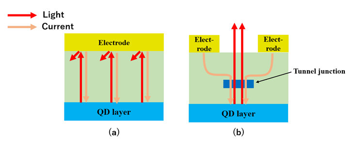
Figure 3 (a) Without a tunnel junction, current flows toward the bottom of the electrode and excites the quantum dot; however, the electrode obstructs light extraction. (b) In the presence of a tunnel junction, the current path can be redirected electrode-free regions, facilitating light extraction.
Threshold Current
The threshold current of a semiconductor laser refers to the minimum current required to initiate stable lasing. In a semiconductor laser, light is generated by passing current through it. For this light to be amplified in a laser, the increase in light intensity inside the chip must exceed the loss of light. The threshold current is the current required to satisfy this condition. The threshold current depends on the material properties, structure, and temperature. For instance, if the efficiency of converting current into light is improved or the loss of light is reduced via superior materials or designs, the threshold current decreases. Quantum dots increase the efficiency of converting current into light. A low threshold current contributes to reducing power consumption and improving the lifetime of devices and is therefore considered important in application fields that require stability and low power consumption.
Technical Contact
AKAHANE Koichi
Optical Access Technology Laboratory
Photonic ICT Research Center
Network Research Institute
E-mail: akahane nict.go.jp
nict.go.jpYAMAMOTO Naokatsu
Advanced ICT Device Laboratory
Network Research Institute
E-mail: naokatsunict.go.jp
nict.go.jpMedia Contact
Press Office
Public Relations Department
E-mail: publicitynict.go.jp
nict.go.jp