Researchers at NICT and Tokyo University of Agriculture and Technology (TUAT) demonstrate a vertical Ga2O3 metal-oxide-semiconductor field-effect transistor (MOSFET) that adopts an all-ion-implanted process for both n-type and p-type doping, paving the way for new generations of low-cost and highly-manufacturable Ga2O3 power electronic devices.
Power electronics is concerned with the regulation and conversion of electric power in such applications as motor drives, electric vehicles, data centers, and the grid. Power electronic devices, namely rectifiers (diodes) and switches (transistors), form the core components of power electronic circuits. Today, power devices made of silicon (Si) are the mainstream but they are approaching fundamental performance limitations, rendering the commercial power systems bulky and inefficient. A new generation of power devices based on the wide-bandgap semiconductor — gallium oxide (Ga2O3) — is expected to revolutionize the power electronics industry. Ga2O3 promises dramatic reductions in the size, weight, cost, and energy consumption of power systems by increasing both the power density and power conversion efficiency at the device level. 
The groundbreaking demonstration of the first single-crystal Ga2O3 transistor by NICT in 2011 galvanized intensive international research activities into the science and engineering of this new oxide semiconductor [1]. For the past several years, the development of Ga2O3 transistors has focused on a lateral geometry. However, lateral devices are not amenable to the high currents and high voltages required for many applications owing to large device areas and reliability issues arising from self-heating and surface instabilities. In contrast, the vertical geometry allows for higher current drives without having to enlarge the chip size, simplified thermal management, and far superior field termination. The properties of a vertical transistor switch are engineered by introducing two types of impurities (dopants) into the semiconductor — n-type doping, which provides mobile charge carriers (electrons) to carry electrical current when the switch is in the on-state; and p-type doping, which enables voltage blocking when the switch is in the off-state. A group at NICT led by Masataka Higashiwaki has pioneered the use of Si as an n-type dopant in Ga2O3 devices, but the community has long struggled to identify a suitable p-type dopant. Earlier this year, the same group published on the feasibility of nitrogen (N) as a p-type dopant [2]. Their latest accomplishment involves integrating Si and N doping to engineer a Ga2O3 transistor for the first time, through a high energy dopant introduction process known as ion implantation.
“Our success is a breakthrough development that promises a transformational impact on Ga2O3 power device technology,” said Higashiwaki, Director of the Green ICT Device Advanced Development Center at NICT. “Ion implantation is a versatile fabrication technique widely adopted in the mass production of commercial semiconductor devices such as Si and silicon carbide (SiC) MOSFETs. The demonstration of an all-ion-implanted vertical Ga2O3 transistor greatly enhances the prospects for Ga2O3-based power electronics.”
This study, published December 3 in the IEEE Electron Device Letters as an early access online paper and scheduled to appear in the January 2019 issue of the journal, builds on an earlier one in which a different acceptor dopant was used [3]. “We initially investigated magnesium for p-type doping, but this dopant failed to deliver its expected performance since it diffuses significantly at high process temperatures,” said Man Hoi Wong, a researcher of the Green ICT Device Advanced Development Center and the lead author of the paper. “Nitrogen, on the other hand, is much more thermally stable, thereby creating unique opportunities for designing and engineering a variety of high-voltage Ga2O3 devices.”
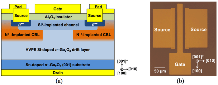
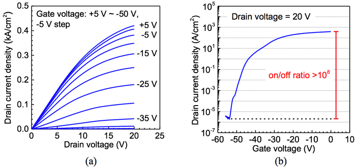
The Ga2O3 base material used for fabricating the vertical MOSFET was produced by a crystal growth technique called halide vapor phase epitaxy (HVPE). Pioneered by Profs. Yoshinao Kumagai and Hisashi Murakami at TUAT, HVPE is capable of growing single-crystal Ga2O3 films at high speeds and with low impurity levels [4]. Three ion implantation steps were performed to form the n-type contacts, n-type channel, and p-type current blocking layers (CBLs) in the MOSFET (Fig. 1). The device showed decent electrical properties including an on-current density of 0.42 kA/cm2, a specific on-resistance of 31.5 mΩ·cm2, and a high drain current on/off ratio larger than eight orders of magnitude (Fig. 2). Further improvements in its performance can be readily achieved with improved gate dielectric quality and optimized doping schemes.
Fig. 1  (a) Cross-sectional schematic and (b) plan-view optical micrograph of the vertical Ga2O3 MOSFET.
Fig. 1 (a) Cross-sectional schematic and (b) plan-view optical micrograph of the vertical Ga2O3 MOSFET.
Fig. 2  (a) DC output and (b) transfer characteristics of the vertical Ga2O3 MOSFET.
Fig. 2 (a) DC output and (b) transfer characteristics of the vertical Ga2O3 MOSFET.
According to Higashiwaki and Wong, “Vertical power devices are the strongest contenders to combine currents over 100 A with voltages over 1 kV — the requirements for many medium- and high-power industrial and automotive electric power systems.” The technological impact of Ga2O3 will be substantially bolstered by the availability of melt-grown native substrates — one of the key enablers of the silicon industry that dominates the global semiconductor market with an annual revenue of several hundred billion U.S. dollars. “The commercialization of vertical SiC and gallium nitride (GaN) power devices has, to a certain extent, been hindered by the high cost of substrates. For Ga2O3, the high quality and large size of native substrates offer this rapidly emerging technology a unique and significant cost advantage over the incumbent wide-bandgap SiC and GaN technologies,” the researchers explained.
This work was partially supported by Council for Science, Technology and Innovation (CSTI), Cross-ministerial Strategic Innovation Promotion Program (SIP), “Next-generation power electronics” (funding agency: New Energy and Industrial Technology Development Organization).

Publication Information

Journal: IEEE Electron Device Letters
Title: Current Aperture Vertical β-Ga2O3 MOSFETs Fabricated by N- and Si-Ion Implantation Doping
Authors: Man Hoi Wong, Ken Goto, Hisashi Murakami, Yoshinao Kumagai, and Masataka Higashiwaki
DOI: 10.1109/LED.2018.2884542

References

[1] M. Higashiwaki, K. Sasaki, A. Kuramata, T. Masui, and S. Yamakoshi, “Gallium oxide (Ga2O3) metal-semiconductor field-effect transistors on single-crystal β-Ga2O3 (010) substrates,” Appl. Phys. Lett., vol. 100, no. 1, p. 103504, Jan. 2012.
[2] M. H. Wong, C.-H. Lin, A. Kuramata, S. Yamakoshi, H. Murakami, Y. Kumagai, and M. Higashiwaki, “Acceptor doping of β-Ga2O3 by Mg and N ion implantations,” Appl. Phys. Lett., vol. 113, no. 10, p. 102103, Sep. 2018.
[3] M. H. Wong, K. Goto, Y. Morikawa, A. Kuramata, S. Yamakoshi, H. Murakami, Y. Kumagai, and M. Higashiwaki, “All-ion-implanted planar-gate current aperture vertical Ga2O3 MOSFETs with Mg-doped blocking layer,” Appl. Phys. Express, vol. 11, no. 6, p. 064102, Jun. 2018.
[4] H. Murakami, K. Nomura, K. Goto, K. Sasaki, K. Kawara, Q. T. Thieu, R. Togashi, Y. Kumagai, M. Higashiwaki, A. Kuramata, S. Yamakoshi, B. Monemar, and A. Koukitu, “Homoepitaxial growth of β-Ga2O3 layers by halide vapor phase epitaxy,” Appl. Phys. Express, vol. 8, no. 1, p. 015503, Jan. 2015. 

Technical Contact

Masataka Higashiwaki
Green ICT Device Advanced Development Center
Advanced ICT Research Institute
National Institute of Information and Communications Technology

Tel: +81-42-327-6092

E-mail: mhigashi-atmark-nict.go.jp

Yoshinao Kumagai
Department of Applied Chemistry
Tokyo University of Agriculture and Technology
Tel: +81-42-388-7469

E-mail: 4470kuma-atmark-cc.tuat.ac.jp

Media Contact

Sachiko Hirota
Press Office
Public Relations Department
National Institute of Information and Communications Technology

Tel: +81-42-327-6923

E-mail: publicity-atmark-nict.go.jp

Public Relations and Endowment Office
General Affairs Office
General Affairs Division
Tokyo University of Agriculture and Technology

Tel: +81-42-367-5930

E-mail: koho2-atmark-cc.tuat.ac.jp